I. 2D Materials for Advanced Devices: Direct Growth by Scalable Methods
A central problem in the development of devices based on 2 dimensional materials is the controlled direct growth of such films on suitable substrates by industrially practical and scalable methods. Our focus is on the direct growth of graphene, hexagonal BN (h-BN) and graphene/h-BN heterostructures on device-suitable substrates for spintronic and advanced electronic applications. Experiments with transition metal dichalcogenides are in progress. Current collaborations involve investigators at UNL, UMN, U Wisc., Caltech, SUNY-Buffalo and elsewhere. Recent highlights include:
Ø
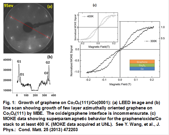 The layer-by-layer growth of high
quality (domain size > 1800 Å) graphene on Co3O4(111)/Co(0001)
by molecular beam epitaxy (MBE) [1]. This results in significant grapheneàoxide charge
transfer and synergistic magnetic properties for the graphene/oxide/Co stack:
superparamagnetism to > 400 K [2]. Such phenomena (Fig. 1) are consistent
with substrate spin-induced polarization of graphene charge carriers, with
potential device implications.
The layer-by-layer growth of high
quality (domain size > 1800 Å) graphene on Co3O4(111)/Co(0001)
by molecular beam epitaxy (MBE) [1]. This results in significant grapheneàoxide charge
transfer and synergistic magnetic properties for the graphene/oxide/Co stack:
superparamagnetism to > 400 K [2]. Such phenomena (Fig. 1) are consistent
with substrate spin-induced polarization of graphene charge carriers, with
potential device implications.
Ø 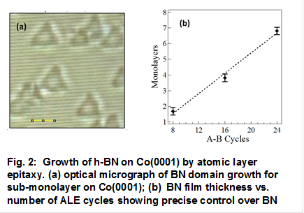 The layer-by-layer growth of
h-BN(0001) on Co(0001) by atomic layer epitaxy [3]. Co/BN/Co
heterojunctions with 5-8 BN layers are of great interest for spin filters, with
predicted tunneling magnetoresistance values >> 1000 %. We are currently
producing such structures (Fig. 2) for transport measurements.
The layer-by-layer growth of
h-BN(0001) on Co(0001) by atomic layer epitaxy [3]. Co/BN/Co
heterojunctions with 5-8 BN layers are of great interest for spin filters, with
predicted tunneling magnetoresistance values >> 1000 %. We are currently
producing such structures (Fig. 2) for transport measurements.
Ø
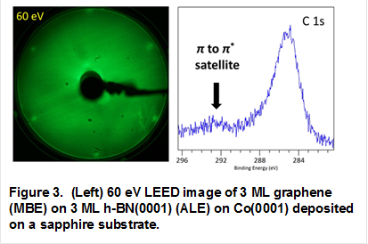 The direct growth of graphene by MBE
on h-BN(0001).
Fig 3. (left) shows a LEED image of 3 ML graphene on 3 ML h-BN(0001) on
Co(0001). The 60 eV LEED data indicate that the Co, BN, and graphene lattices
are in precise azimuthal registry—a critical factor for advanced spin and electronic
tunneling devices. Fig. 3 (right) shows XPS data indicating that the hexagonal
C layer in the LEED exhibits the expected asymmetric C 1s peak and associated
πàπ* shakeup feature expected for
graphene. The ability to directly grow graphene/BN heterostructures with
varied graphene and BN layer thicknesses opens the way to a variety of
spintronic and ultrahigh frequency electronic devices based on such
heterostructures. Such heterostructures are now being produced for
nanoscale-transport measurements.
The direct growth of graphene by MBE
on h-BN(0001).
Fig 3. (left) shows a LEED image of 3 ML graphene on 3 ML h-BN(0001) on
Co(0001). The 60 eV LEED data indicate that the Co, BN, and graphene lattices
are in precise azimuthal registry—a critical factor for advanced spin and electronic
tunneling devices. Fig. 3 (right) shows XPS data indicating that the hexagonal
C layer in the LEED exhibits the expected asymmetric C 1s peak and associated
πàπ* shakeup feature expected for
graphene. The ability to directly grow graphene/BN heterostructures with
varied graphene and BN layer thicknesses opens the way to a variety of
spintronic and ultrahigh frequency electronic devices based on such
heterostructures. Such heterostructures are now being produced for
nanoscale-transport measurements.
Current work is focused on the fabrication of BN and graphene/BN heterostructures for device transport measurements, and the expansion of these growth efforts to other oxide substrates.
REFERENCES
[1] M. Zhou, F.L. Pasquale, P.A. Dowben, A. Boosalis, M. Schubert, V. Darakchieva, R. Yakimova, J.A. Kelber. Direct graphene growth on Co3O4(111) by molecular beam epitaxy. J Phys: Cond Matt. 24 (2012) 072201.
[2] Y. Wang, L. Kong, F.L. Pasquale, Y. Cao, B. Dong, I. Tanabe, C. Binek, P.A. Dowben, J.A. Kelber. Graphene mediated domain formation in exchange coupled graphene/Co3O4(111)/Co(0001) trilayers. J Phys : Cond Matt. 25 (2013) 472203.
[3] J. Beatty, Y. Cao, I. Tanabe, M. S. Driver, P. A. Dowben and J. A. Kelber, Atomic layer-by-layer depostion of h-BN(0001) on cobalt: a building block for spintronics and graphene electronics Mat. Res. Express 1 (2014) 046410