Research Thrusts
Research in the Kelber group is currently focused on the development of emerging or novel materials in three areas:
I. 2D Materials: Direct growth for Advanced Devices
II. Ultrathin Magnetic Oxide Films for Spintronics Applications
III. Boron Carbide/polymer composites for neutron detection
These efforts focus on the formation of thin films and monolayers by various methods, including:
I. Molecular Beam Epitaxy
II. Plasma-Enhanced Chemical Vapor Deposition
III. Atomic Layer Deposition
Typically, film deposition and characterization are done under controlled conditions, without sample exposure to ambient. This permits a more detailed understanding of growth processes. Film characterization methods include core and valence band photoemission, Auger electron spectroscopy, low energy electron diffraction, FTIR and other methods. Funding agencies include CSPIN, a MARCO/DARPA STARnet Center, NSF, and the US DTRA.
Research Capabilities
Research focusses on formation and modification of thin films and surfaces in complex environments. Therefore, capabilities focus on sample transfer between deposition environment and ultra-high vacuum surface analysis without sample exposure to ambient. Experimental resources include the following systems:
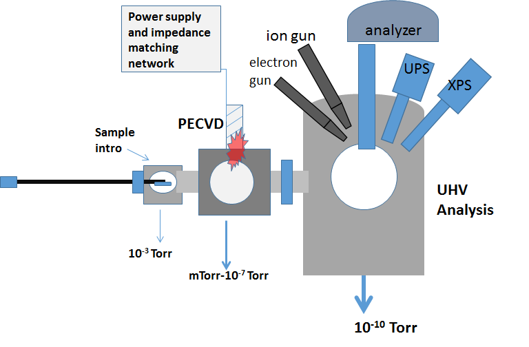
Plasma enhanced chemical vapor deposition and core and valence band photoemission (XPS and UPS). This includes a home built chamber for inductively coupled plasma chemical vapor deposition with dual mass flow controllers, and an analysis chamber equipped with a 140 mm mean radius hemispherical analyzer with channel plate detector, dual anode x-ray source, plasma-based ultraviolet source, and ion sputter deposition. This system is capable of deposition of films with thicknesses ranging from 5 Å to > 5000 Å.
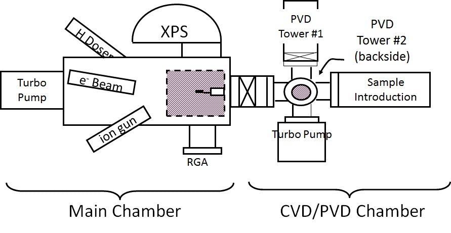
Dual magnetron sputter deposition, chemical vapor deposition and XPS. This system includes a chamber with dual magnetrons for sputter deposition of layered or alloyed films, and an analysis chamber with capabilities for XPS with a 100 mm mean radius analyzer with channeltron detector, dual anode x-ray source and ion sputter gun.
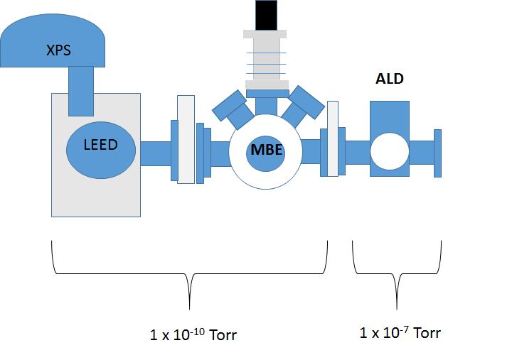
Atomic layer deposition/molecular beam epitaxy/LEED and XPS. This system includes separate chambers for atomic layer deposition at temperatures between 300 K and 1300 K, molecular beam epitaxy with a quad source electron beam evaporator, and surface analysis with a 100 mm mean radius hemispherical analyzer/multichanneltron detector and dual anode x-ray source for XPS, and a reverse view LEED system.
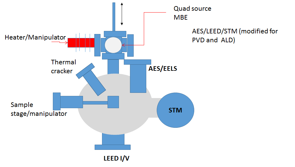
Molecular beam epitaxy, Auger and Electron Energy Loss Spectroscopy, Scanning Tunneling Microscopy, and LEED I(V) This system contains a quad source ebeam evaporator with Ir filaments for MBE operation in reactive environments, a double-pass cylindrical mirror analyzer with concentric electron gun for Auger and EELS, a video LEED I(V) system, and an ambient temperature STM.
Additional resources within the Kelber group include:
1. A potentiostat and 3 electrode cell for electrochemistry
2. An atomic force microscope
3. A dedicated magnetron sputter deposition chamber
4. A FTIR spectrometer
5. A tube furnace.
6. A Magneto-Optic Kerr Effect (MOKE) measurement facility (under construction)